Hardware integration guide
PN7160 MINI V1 -- I2C
Connect power and host signals, select the I2C address, and integrate the antenna and module into your product.
1. Module connections
Connect VCC to a 3.3–5.5 V supply and GND to the host ground. Connect SDA and SCL to the host I2C bus, IRQ to a host input and VEN to a host output. Match the signal labels on the module; do not identify pins by cable color.
The dot beside the six-pin connector marks Pin 1 (SDA). See the connector-orientation images and pin table before connecting. A six-pin host cable is not included.
2. Power design
2.1 Supply and wiring
| Item | Integration requirement |
|---|---|
| Input voltage | 3.3–5.5 V at the module VCC/GND connection, including source tolerance and ripple. |
| Supply capacity | At least 300 mA available to the module. A 500 mA or higher-rated source provides additional margin; budget other system loads separately. |
| Signal levels | 3.3 V host logic on SDA, SCL, IRQ and VEN, regardless of the VCC supply voltage. |
| Power routing | Keep VCC and GND connections short and use a stable, low-impedance supply. Check the voltage at the module connector during operation. |
| Decoupling | Local decoupling is built in. Any additional host-side bulk capacitance depends on the supply, cable and other loads; no universal value is specified. |
For approximate operating-current observations with the supplied antennas, see the datasheet current reference.
2.2 Software power configuration
Select the library power configuration for the actual supply before configuring RF operation. The following examples cover 3.3 V and 5.0 V supplies.
| Supply | Arduino configuration | How to apply |
|---|---|---|
| 3.3 V | setPn7160FixedVbat3V3(true) | Call before configureSettings(). This is used in the supplied ESP32-S3 quick-start example. |
| 5.0 V | setPn7160FixedVbat3V3(false) | Call before configureSettings() to select the normal external-5 V configuration. |
Fully disconnect and restore module power after changing the supply configuration. For other supply designs within 3.3–5.5 V, confirm the appropriate software configuration with support; see the Software Guide.
3. I2C interface
- Use 3.3 V host logic and connect the host and module grounds.
- The module includes 4.7 kΩ pull-ups on SDA and SCL to the 3.3 V logic supply. Include them when checking the combined pull-up resistance if the host also has pull-ups.
- Keep SDA and SCL wiring short and close to a ground connection. Check timing at the actual cable length and bus capacitance.
- Use 400 kHz for normal integration. Standard-mode at 100 kHz is also supported.
- Connect IRQ to an interrupt-capable host input for data-ready notification.
Logic-level compatibility
Use the digital signal-level table to check the host interface. SDA and SCL require a HIGH input of at least 70% of the module logic supply and a LOW input no higher than 30%. At a 3.3 V logic supply these are 2.31 V and 0.99 V, respectively. Do not substitute the external VCC voltage in these calculations.
VEN has separate thresholds: HIGH from 1.1 V, LOW up to 0.4 V; its input must not exceed the actual module VCC. Continue to use a 3.3 V host output for normal connection. IRQ drives a host input; its output-level limits apply at a source or sink current below 3 mA.
These DC limits follow the PN7160 electrical specification, Rev. 4.2, Tables 48, 49 and 59. They do not replace timing checks with the final wiring and pull-ups.
4. IRQ, VEN and DWL
| Signal | Function | Connection / use |
|---|---|---|
| IRQ | Active-high data-ready output | Connect to a host input. Read pending NCI data until IRQ is released. |
| VEN | Enable/reset input | Drive low for reset and high for operation. The ELECHOUSE library handles the reset sequence during initialization. |
| DWL | Firmware-maintenance pad | Leave unconnected during normal use. Use only with a supported firmware-maintenance procedure. |
5. I2C address selection
Use the solder pads marked ADR0 and ADR1 on the module. An open pad selects logic 0; bridging the two halves of a pad with solder selects logic 1. Both pads are open as supplied.
| ADR1 | ADR0 | 7-bit I2C address |
|---|---|---|
| Open (0) | Open (0) | 0x28 — factory default |
| Open (0) | Soldered (1) | 0x29 |
| Soldered (1) | Open (0) | 0x2A |
| Soldered (1) | Soldered (1) | 0x2B |
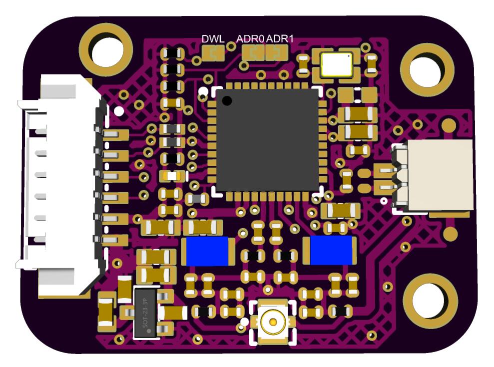
- Disconnect all power before soldering.
- Bridge only the selected ADR pad or pads. Leave the DWL maintenance pad unchanged.
- Check for unintended solder bridges.
- Set the host software to the corresponding 7-bit address.
- Reconnect power and initialize the module.
To restore the default address, remove the solder bridges from both ADR pads with power disconnected, then set the host address to 0x28 and power up again.
6. RF and antenna integration
| Antenna connection | Connector | Selection guidance |
|---|---|---|
| Connector 2 — preferred | ST1.0, 1.0 mm-pitch, 2-pin wire-to-board | Use the matching two-wire antenna assembly for low connection loss. |
| Connector 1 — alternative | IPEX4 | Use a matching shielded coaxial lead. Longer leads reduce reading distance; check performance with the final cable length. |
6.1 Antenna options and reading-distance reference
The standard package contains both 50 × 40 mm and 25 × 10 mm antennas. The 100 × 160 mm antenna is available separately and is not included in the standard package. Antenna lead length is 10 cm.
| Antenna size | Package / availability | S70 | ISO/IEC 15693 |
|---|---|---|---|
| 25 × 10 mm | Included as standard | 2.9 cm | 6.5 cm |
| 50 × 40 mm | Included as standard | 5.0 cm | 14.0 cm |
| 100 × 160 mm | Optional; sold separately | 5.6 cm | 12.0 cm |
These are reference observations, not guaranteed minimum distances. Results depend on the card or tag, supply, orientation, antenna connection and surrounding materials. Other antenna sizes are available by customization; contact service@elechouse.com with your installation space and application requirements.
Test conditions: 5 V supply, ST1.0 connection (connector 2), and a 10 cm antenna lead. Hold the card parallel to the antenna and determine the maximum reading distance. S70 results use an 85 × 55 mm MIFARE S70 PVC card; ISO/IEC 15693 results use an 85 × 55 mm ICODE SLIX2 card.
6.2 Installation guidance
- Use a supplied or supported antenna assembly. Avoid changing the lead length without checking reading performance.
- Keep metal, batteries, displays, ground planes and cable loops away from the active antenna area.
- Check reading performance in the final enclosure with its mounting hardware and nearby wiring in place.
- Keep antenna connections mechanically secure and leave room for the plug and cable bend.
- Disconnect power before changing antennas and follow ESD handling precautions.
7. Mechanical integration
| Item | Value / integration guidance |
|---|---|
| PCB outline | 26.937 × 20.066 mm nominal; standard routed-profile tolerance reference: ±0.20 mm. |
| PCB thickness | 1.60 mm nominal; standard fabrication tolerance reference: ±0.16 mm (±10%), or 1.44–1.76 mm. |
| Maximum module thickness | 5.5 mm. Allow additional space for plugs and cables. |
| Mounting holes | 3 plated through-holes, Ø2.11 ± 0.10 mm. |
Use the STEP model and DXF drawing for nominal mounting-hole positions and enclosure design. Allow for the outline and thickness tolerances above, together with space for the selected plugs, cable bends and insertion/removal.
8. Environment and ESD
Operate the module from −25°C to +85°C in a non-condensing environment. For storage, aim for +5°C to +30°C and 40–60% RH in ESD-protective packaging. These are recommended warehouse conditions, not extreme storage ratings.
- Handle the bare module with ESD precautions and protect it from moisture, conductive contamination and corrosive gases.
- Provide suitable host-side protection for connectors exposed outside the enclosure.
- Keep fast digital signals and switching-power circuits away from the antenna.
- Check emissions, immunity and RF performance in the completed host product; module integration does not certify the end product.
No module-level ESD rating is specified. Use ESD handling precautions and assess protection requirements for the completed host product.
9. First-start checklist
- Check the module version and identify the connector signals from the module labels.
- With power disconnected, connect one antenna and the six host signals.
- Check VCC polarity, common ground and 3.3 V host logic.
- Match the software I2C address to the ADR0/ADR1 pad settings; use 0x28 for the factory default. Set the host I2C clock to the recommended 400 kHz.
- Select the software power configuration for the actual supply voltage.
- Apply power and check VCC at the module connector and the SDA/SCL idle levels.
- Run the supplied example, confirm initialization and read the firmware version.
- Test the required card types using the selected antenna.
- Repeat the reading test after installation in the final enclosure.