Product datasheet
PN7160 MINI V1 -- I2C
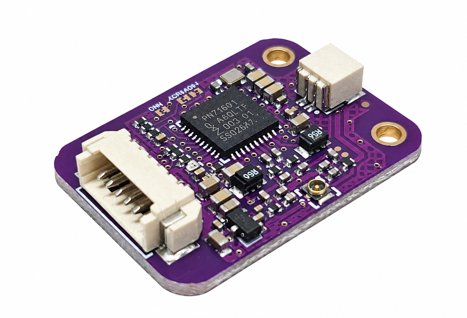
Compact NFC module with a six-pin host connection and two included external antennas.
1. Product overview
The ELECHOUSE PN7160 MINI V1 adds NFC communication to embedded systems through an I2C host interface. The six-pin connection provides power, data, interrupt and enable/reset signals.
Key features
- 13.56 MHz NFC operation based on the NXP PN7160 controller.
- NFC-A/B/F/V support, including ISO/IEC 14443, ISO/IEC 15693, FeliCa and MIFARE workflows.
- Reader/writer and card-emulation modes, subject to controller firmware and host software support.
- 3.3–5.5 V supply input and 3.3 V host logic.
- Default I2C address: 0x28 (7-bit).
- 26.937 × 20.066 mm PCB with three mounting holes.
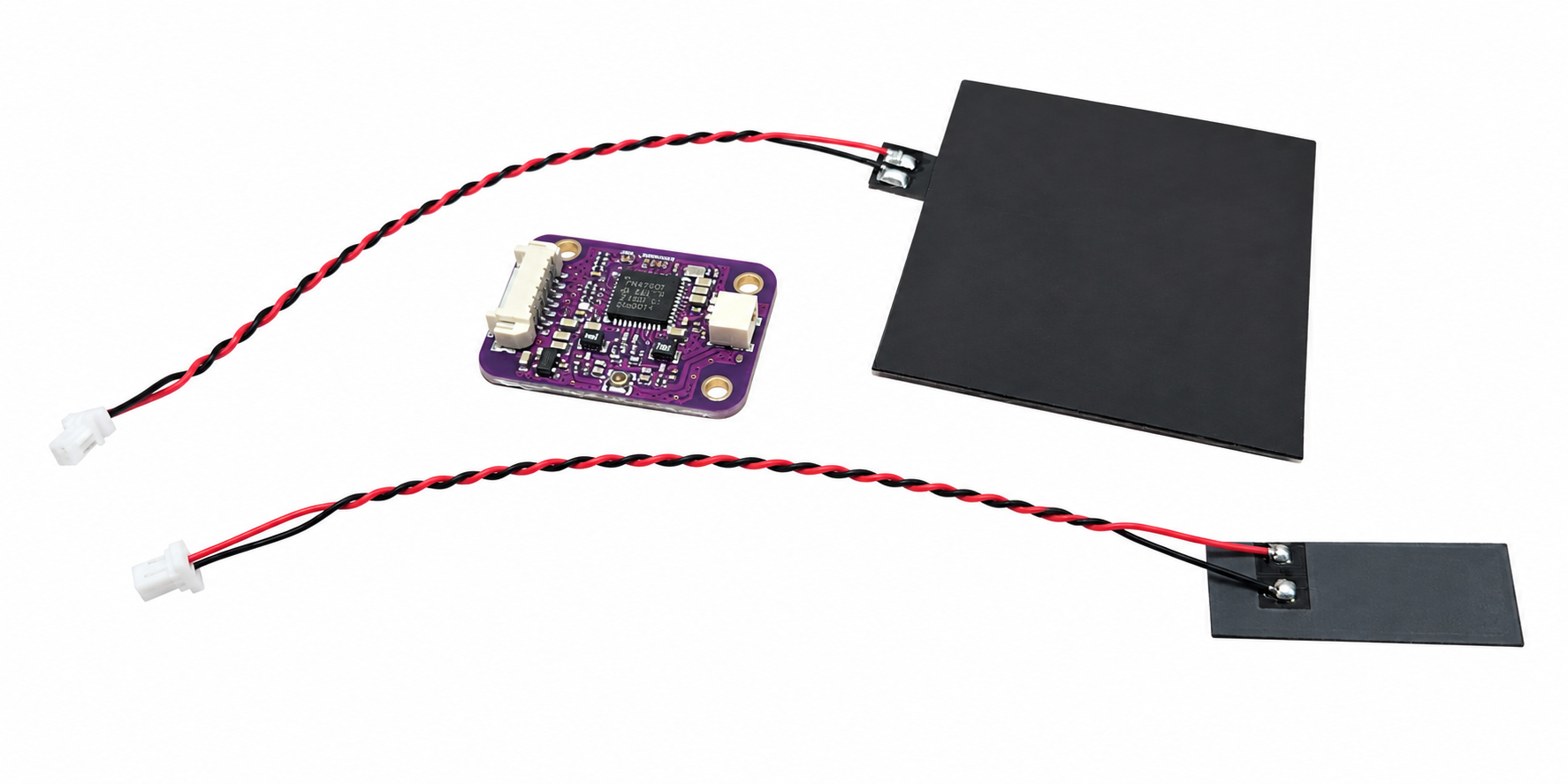
- Both 50 × 40 mm and 25 × 10 mm antennas included.
- Arduino library and ESP32-S3 quick-start example available.
2. Electrical and environmental specifications
| Parameter | Value | Notes |
|---|---|---|
| VCC input operating range | 3.3–5.5 V | Specified at the module connector, including supply tolerance and ripple. Do not exceed 5.5 V. |
| Host logic | 3.3 V | Use 3.3 V logic for SDA, SCL, IRQ and VEN. |
| Recommended supply capacity | At least 300 mA available to the module | A 500 mA or higher-rated source provides additional margin. Budget other system loads separately. |
| Operating temperature | −25°C to +85°C | Use in a non-condensing environment. |
| Recommended storage conditions | +5°C to +30°C; 40–60% RH | Warehouse guidance, not an extreme storage rating. Keep dry in ESD-protective packaging. |
Operating-current reference
| Antenna | Recorded average current | Test condition |
|---|---|---|
| 25 × 10 mm | Approximately 67 mA | Nominal 5 V supply, card present. |
| 50 × 40 mm | Approximately 108 mA | Nominal 5 V supply, card present. |
These values are reference observations, not maximum-current ratings. Current varies with the antenna and operating mode. Startup and peak current are not specified.
Handle the bare module using ESD precautions. Protect it from moisture and conductive contamination.
3. Host connector and pinout
The host connector is a 1.25 mm-pitch, single-row, PicoBlade-compatible 6-pin interface. The dot beside the connector identifies Pin 1 (SDA). Use a matching cable and check the signal order before connection. The host cable is not included.
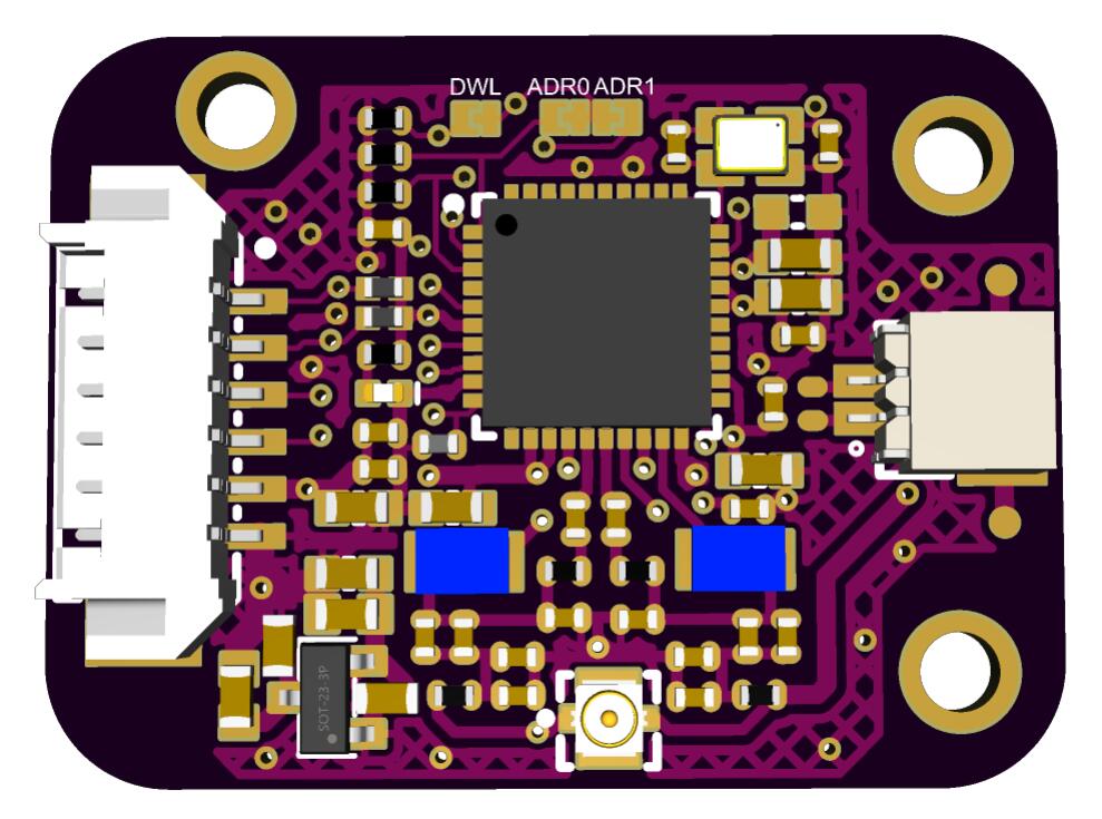
Connecting the host cable
- Disconnect power and locate the dot beside the six-pin connector: Pin 1 is SDA.
- Use a matching 1.25 mm, six-pin cable and check its signal order against the table below.
- Align the keyed plug with the connector housing. Insert it into the side opening without forcing it.
The six-pin host cable is not included. Select a compatible cable.
Signal directions in the table are relative to the module. Do not rely on cable colors to identify pins.
| Pin | Signal | Direction | Function |
|---|---|---|---|
| 1 | SDA | Bidirectional | I2C data. |
| 2 | SCL | Input | I2C clock. |
| 3 | IRQ | Output | Active-high notification that data is available for the host. |
| 4 | VEN | Input | Enable/reset control: high enables the module; low holds it in reset. |
| 5 | VCC | Power | 3.3–5.5 V supply input. |
| 6 | GND | Power | Ground. Connect to the host ground. |
4. Communication and control
| Item | Specification / use |
|---|---|
| Host communication | I2C using the NFC Controller Interface (NCI). IRQ indicates data availability. |
| Default address | 0x28 (7-bit). ADR0 and ADR1 address-selection pads are open as supplied. |
| Address options | 0x28–0x2B, selected using the pads marked ADR0 and ADR1. Open = 0; solder-bridged = 1. See the table below. |
| I2C speeds | 100 kHz Standard-mode and 400 kHz Fast-mode; 400 kHz recommended. Check bus timing with the final wiring and pull-ups. |
| I2C pull-ups | Built-in 4.7 kΩ pull-ups on SDA and SCL to the 3.3 V logic supply. Allow for these if the host also has pull-ups. |
| Firmware-maintenance pad | DWL is for maintenance only. Leave it unconnected during normal use. |
Digital signal levels
All voltages are relative to GND. VIO is the module's nominal 3.3 V logic supply, not the external VCC input. The formulas below use the actual logic-supply voltage; the numerical examples assume VIO = 3.3 V.
| Signal | Parameter | Limits | Conditions / example |
|---|---|---|---|
| SDA, SCL | HIGH input, VIH | 0.7 × VIO to VIO | 2.31–3.30 V at VIO = 3.3 V. |
| SDA, SCL | LOW input, VIL | 0 to 0.3 × VIO | 0–0.99 V at VIO = 3.3 V. |
| VEN | HIGH input, VIH | 1.1 V to VCC | Use a 3.3 V host output for normal connection. Never exceed the actual module VCC. |
| VEN | LOW input, VIL | 0–0.4 V | Holds the module in reset. |
| SDA | LOW output, VOL | 0–0.4 V | Sink current < 3 mA. HIGH is provided by the I2C pull-up. |
| IRQ | HIGH output, VOH | VIO − 0.4 V to VIO | Source current < 3 mA; 2.90–3.30 V at VIO = 3.3 V. |
| IRQ | LOW output, VOL | 0–0.4 V | Sink current < 3 mA. |
Keep SDA and SCL within 0 V to VIO. SCL is an input only; SDA is open-drain. Input voltages between the stated LOW and HIGH ranges do not define a valid logic state. These DC limits do not specify allowable cable length or bus timing.
I2C address selection
Use the ADR0 and ADR1 markings on the module to identify the address-selection pads. Both are supplied open, giving address 0x28. Soldering across the two contacts of an individual pad sets that address bit to 1.
| ADR1 | ADR0 | 7-bit I2C address |
|---|---|---|
| Open (0) | Open (0) | 0x28 — default |
| Open (0) | Solder-bridged (1) | 0x29 |
| Solder-bridged (1) | Open (0) | 0x2A |
| Solder-bridged (1) | Solder-bridged (1) | 0x2B |
- Disconnect power before changing the solder bridges.
- Bridge only the two contacts of each selected pad. Do not join ADR0 to ADR1 or to the nearby DWL pad. Remove the solder bridge to return a bit to 0.
- Check for unintended solder bridges, set the host software to the selected 7-bit address, then reconnect power.
Use the supplied library and the power setting appropriate to the actual supply voltage. Start with the ESP32-S3 Quick Start for a 3.3 V example; see the Software Guide for configuration details.
5. Antennas and reading performance
The standard package includes two antennas: 50 × 40 mm and 25 × 10 mm. A 100 × 160 mm antenna can be purchased separately. Antenna lead length is 10 cm. Other sizes are available by customization; contact us with your installation space and application requirements.
| Antenna size | Supply status |
|---|---|
| 50 × 40 mm | Included as standard. |
| 25 × 10 mm | Included as standard. |
| 100 × 160 mm | Optional; sold separately, not included in the standard package. |
| Other sizes | Custom order; discuss requirements by email. |
Antenna connections
| Connection | Connector type | Selection guidance |
|---|---|---|
| Antenna connector 2 — preferred | ST1.0, 1.0 mm-pitch, 2-pin wire-to-board | Use the matching two-wire antenna assembly. This connection has low connection loss. |
| Antenna connector 1 — alternative | IPEX4 | For an IPEX4 shielded coaxial lead. Longer leads reduce reading distance; check performance with the final cable length. |
Reading distance
| Antenna size | S70 test card | ISO/IEC 15693 test card |
|---|---|---|
| 25 × 10 mm — included | 2.9 cm | 6.5 cm |
| 50 × 40 mm — included | 5.0 cm | 14.0 cm |
| 100 × 160 mm — sold separately | 5.6 cm | 12.0 cm |
Test conditions: 5 V supply; ST1.0 antenna connection (connector 2); 10 cm antenna lead; card held parallel to the antenna while determining the maximum reading distance.
- S70 test card: MIFARE S70, 85 × 55 mm PVC card.
- ISO/IEC 15693 test card: ICODE SLIX2, 85 × 55 mm card.
These maximum observed distances are reference results for the production configuration, not guaranteed minimum distances for every card or installation.
Reading distance depends on the antenna, card/tag, supply, cable length, orientation and nearby materials. Check performance in the final enclosure, particularly near metal.
6. Mechanical dimensions
| Parameter | Value | Notes |
|---|---|---|
| PCB dimensions | 26.937 × 20.066 mm nominal | Standard routed-profile tolerance reference: ±0.20 mm. |
| PCB thickness | 1.60 mm nominal | Standard fabrication tolerance reference: ±0.16 mm (±10%); 1.44–1.76 mm. |
| Maximum module thickness | 5.5 mm | Allow additional space for mating plugs and cables. |
| Mounting holes | 3 × Ø2.11 ± 0.10 mm | Plated through-holes (copper-plated walls). |
Use the STEP model and DXF drawing for nominal mounting-hole positions and enclosure design. Allow for the outline and thickness tolerances above, together with space for the selected plugs, cable bends and insertion/removal.
7. Ordering and package contents
| Ordering code | Version | Availability |
|---|---|---|
PN7160_MINI_I2C | PN7160, I2C | Standard product version. |
The standard package includes the module, a 50 × 40 mm antenna and a 25 × 10 mm antenna, with 10 cm antenna leads. Select one antenna for use. The 100 × 160 mm antenna is sold separately and is not included.
Separate custom order: a PN7161-based version can be made to order and is not held in stock or included in this PN7160 product offer. For requirements, quantities and lead times, email service@elechouse.com. Custom antenna enquiries are also welcome.
Not included: six-pin host cable. Provide a compatible cable for your host connection.
8. Downloads and support
Product and customization enquiries: service@elechouse.com.