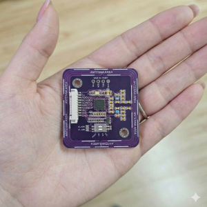
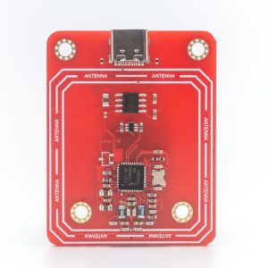
Product Overview
Key Features
- Industrial Power Stability: Equipped with 4x 20uF Capacitors reservoir and a high-speed ME6211 LDO. This design absorbs high-current RF pulses (up to 250mA), preventing voltage dips and ensuring consistent read performance even during continuous high-power transmission.
- Fail-Safe “Hard Reboot” Control: Features a dedicated Chip Enable (CE) pin. This allows the host MCU to physically power-cycle the PN5180 logic core, providing a 100% reliable recovery method from any communication error or state-machine lockup without manual intervention.
- Flexible Logic Voltage (PVDD): The interface logic level is determined by the PVDD pin, supporting the full range from 1.65V to 3.6V (compatible with modern 1.8V MCUs and standard 3.3V ESP32/STM32). Includes an onboard jumper for plug-and-play 3.3V configuration.
- Optimized RF Tuning: The antenna matching circuit is tuned with thermally stable components and optimized damping, eliminating the “hot-dead” drift issue and ensuring stable reading distances across varying temperatures.
Comparison: Which NFC Module is Right for You?
Choosing between the PN5180, the classic PN532, and the newer PN7160 can be difficult. Here is a breakdown to help you decide:
| Feature | PN5180 (This Module) | PN532 | PN7160 |
|---|---|---|---|
| Type | Frontend (RF Transceiver) | Controller | Controller (NCI) |
| Best For | Long Range & Industrial ISO15693 | Hobbyist & Legacy Projects | Android / Linux Integration |
| RF Performance | High (Dynamic Power Control) | Medium | High |
| ISO 15693 Range | Excellent (Best in class) | Limited / Poor | Good |
| Interface | SPI | SPI / I2C / UART | I2C |
| Firmware | External (Library on MCU) | Integrated in Chip | Integrated (NCI Firmware) |
| Why choose it? | Choose this for max range, hardware control, and ISO15693 tags. | Choose this for simple, low-cost prototypes or UART. | Choose this for fast integration with OS-based systems. |
Technical Specifications
- Main Chip: NXP PN5180
- Operating Protocols:
- ISO/IEC 14443 A/B
- ISO/IEC 15693 (ICODE SLIX, SLIX 2)
- ISO/IEC 18092 (NFC P2P)
- FeliCa (JIS X 6319-4)
- Input Voltage (5V Pin): 4.5V – 5.5V (Required for TVDD RF Power)
- Logic Voltage (PVDD): 1.65V – 3.6V (As per NXP Datasheet)
- Host Interface: SPI (up to 7 Mbps) + BUSY line flow control
- Connector: Standard 2.54mm Header
Pinout Description
| Pin Name | Function | Note |
|---|---|---|
| 5V | Power Input | Supplies the RF Transmitter (TVDD). Must be connected. |
| 3V3 | Power Output | 3.3V Output from onboard LDO (Max 500mA). |
| GND | Ground | System Ground. |
| PVDD | Logic Level Ref | Connect to MCU Logic Voltage (e.g., 1.8V or 3.3V). Bridge Jumper to use onboard 3.3V. |
| NSS | SPI Chip Select | Active Low. |
| MOSI | SPI Data In | Master Out Slave In. |
| MISO | SPI Data Out | Master In Slave Out. |
| SCK | SPI Clock | Serial Clock. |
| BUSY | Flow Control | Required. Indicates when the chip is processing. |
| RST | Reset | Standard Soft Reset input. |
| PD/CE | Chip Enable | Hard Power Control. Low = Logic Power OFF; High (by default) = ON. |
Application Note: Logic Level Configuration
The module features a solder jumper (labeled PVDD=3V3) on the back to configure the logic voltage level.
1. Standard 3.3V MCUs (ESP32, Arduino Uno/Mega)
- Action: Solder/Bridge the PVDD=3V3 Jumper.
- Result: This internally connects PVDD to the onboard 3.3V regulator. No external wiring to the PVDD pin is needed.
2. 1.8V MCUs (Modern STM32, ESP32-S3 1.8V Mode)
- Action: Keep the PVDD=V3 Jumper OPEN (Default).
- Result: Connect your MCU’s 1.8V power rail to the PVDD pin. This ensures all SPI and GPIO signals match your MCU’s voltage level perfectly without level shifters.
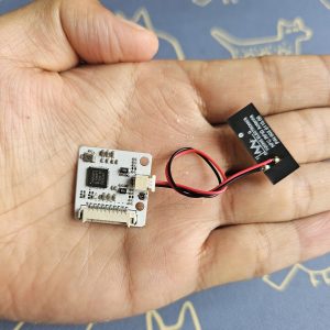
Package Includes
- 1x PN5180 Industrial NFC Module